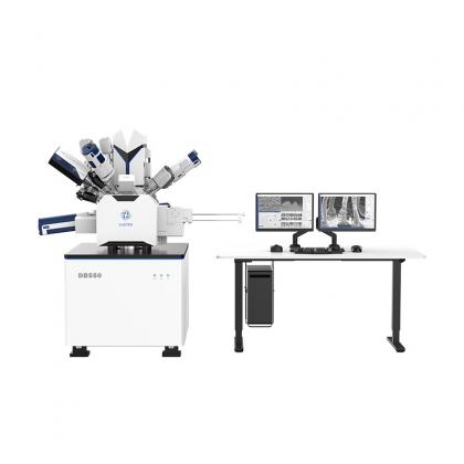



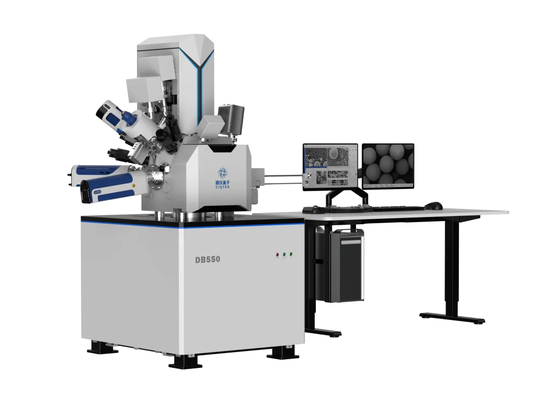
Двухлучевой ионно-лучевой сканирующий электронный микроскоп CIQTEK DB550 объединяет в себе высокоразрешающую электронную визуализацию и прецизионную обработку ионным пучком на одной платформе.
Компания CIQTEK подтвердила свою эффективность. Сканирующий электронный микроскоп DB550 с фокусированным ионным пучком (FIB-SEM) на реальных образцах чипов, изготовленных по 5-нм технологическому процессу, Демонстрация подготовки образцов для ПЭМ-анализа, готовых к производству, с неповрежденными структурами ребер, нулевой аморфизацией и четко различимыми слоями пленки. Результаты подтверждают, что DB550 отвечает самым высоким требованиям современных лабораторий анализа отказов полупроводников, работающих на переднем крае технологических процессов.
В передовых исследованиях и производстве микросхем два инструмента имеют первостепенное значение. Трансмиссионный электронный микроскоп (ТЭМ) позволяет наблюдать структуры на атомном уровне. Но прежде чем начать исследование, необходим образец, достаточно тонкий для прохождения электронов. Именно здесь на помощь приходит двухлучевой сканирующий электронный микроскоп с ионно-лучевой обработкой (FIB-SEM). Это высокоточный цех, где подготавливаются такие сверхтонкие образцы.
Представляем DB550: единая платформа для получения изображений и обработки наноразмерных данных.
Он CIQTEK DB550 FIB-SEM Эта платформа объединяет две мощные возможности. С одной стороны, сканирующий электронный микроскоп (СЭМ) обеспечивает получение изображений поверхности с высоким разрешением. С другой стороны, сфокусированный ионный пучок (СИБ) выполняет удаление наноматериалов с хирургической точностью. Вместе они преодолевают разрыв между наблюдением и изготовлением в размерах, измеряемых миллиардными долями метра.
В основе DB550 лежит низковольтная электронная колонка высокого разрешения в сочетании с запатентованной технологией CIQTEK Ионная колонка "Чэнъин" Разработанная полностью собственными силами, колонна Ченгин является движущей силой системы, обеспечивающей возможности наноразмерной резки и травления. Компания CIQTEK контролирует весь процесс проектирования и производства этого важнейшего компонента.
Проблема 5 нм: почему подготовка образцов усложняется на каждом узле.
В 5 нм и ниже Архитектура микросхем основана на полевых транзисторах с ребрами (FinFET), ширина и шаг ребер которых измеряются всего в несколько нанометров. DB550 разработан для выполнения полного цикла подготовки образцов для этих требовательных технологических узлов. Он начинается с высокотоковая черновая резка для быстрого удаления основного материала и достижения целевой области. Затем происходит переход к низковольтная тонкая полировка истончить образец до размеров, подходящих для просвечивающей электронной микроскопии, не повреждая при этом хрупкие структуры под ним.
Проверка методом просвечивающей электронной микроскопии: доказательство на изображении.
CIQTEK На технологическом стенде DB550 был подготовлен образец чипа, изготовленного по 5-нм техпроцессу, и перенесен на просвечивающий электронный микроскоп для характеризации. Результаты говорят сами за себя.
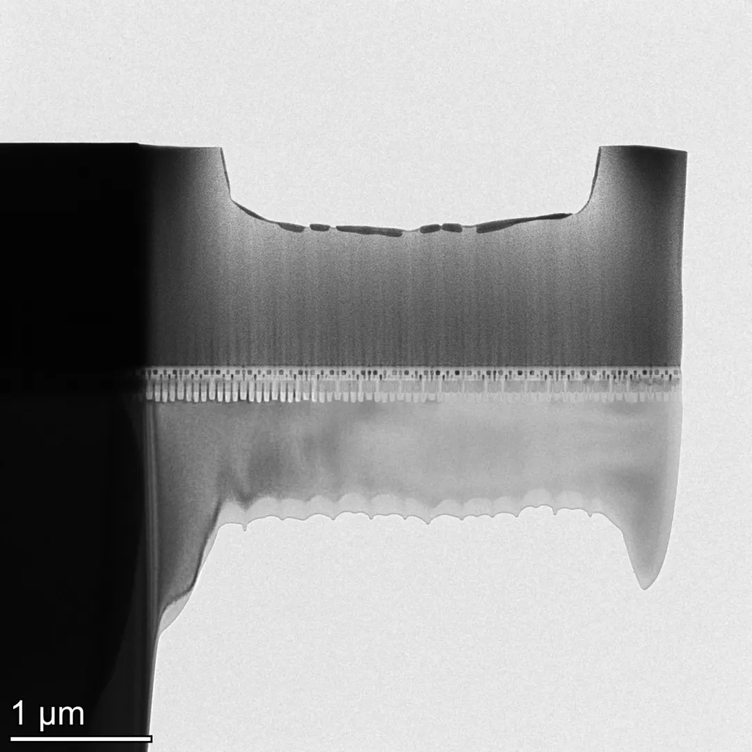
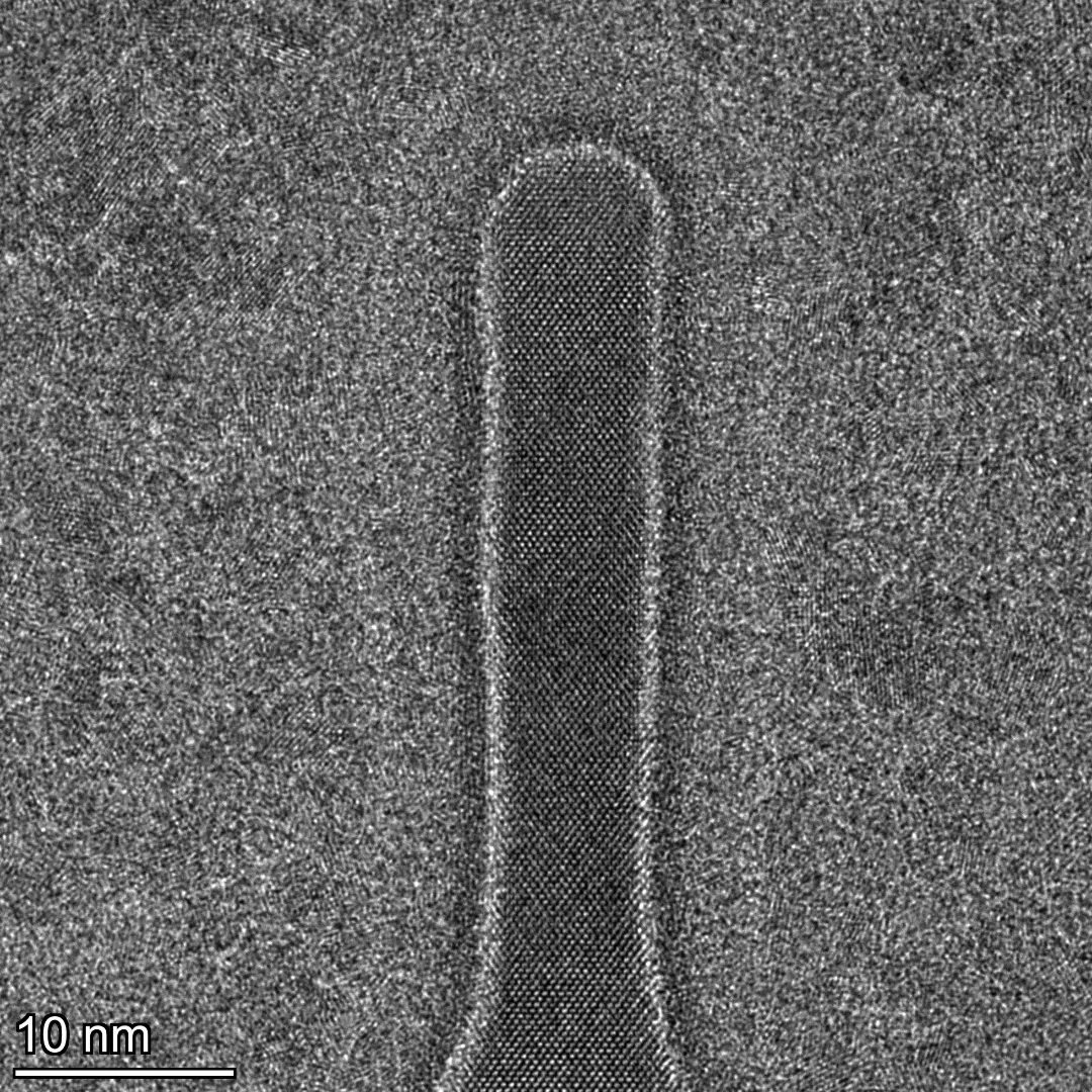
TEM-характеризация образца чипа размером 5 нм, изготовленного на DB550, показывает наличие неповрежденных реберных структур с четкими, хорошо сформированными пленочными слоями и отсутствием повреждений, вызванных аморфизацией.
Изображения, полученные с помощью просвечивающей электронной микроскопии, показали, что Конструкция плавников осталась полностью неповрежденной. После подготовки методом ионно-лучевой обработки (FIB) аморфизации кристаллической решетки кремния обнаружено не было. Наблюдались отдельные слои пленки. четкий и резко очерченный в поперечном сечении TEM. Эти результаты подтверждают эффективность двухлучевой подготовки образцов на приборе DB550 на самых передовых технологических узлах.
Разработан для надежности, создан для долгой службы
Электронные микроскопы являются основным инструментом в лабораториях по анализу отказов полупроводниковых компонентов. Компания CIQTEK разработала DB550 с нуля, охватив весь технологический стек, начиная с... от базового оборудования до лежащих в его основе алгоритмов Фирменная ионная колонка Чэнъин, электронная оптика, механика платформы и программное обеспечение управления разработаны и оптимизированы как единая интегрированная система.
Полное владение проектом повышает устойчивость цепочки поставок. Каждый критически важный компонент поставляется через контролируемый конвейер разработки CIQTEK. Для полупроводниковых лабораторий, которые зависят от бесперебойной работы оборудования для анализа выхода годной продукции и расследования отказов, эта предсказуемость имеет большое значение.
Компания CIQTEK обеспечивает поддержку DB550 следующим образом: непрерывная, надежная и оперативная техническая поддержка Компания также оказывает техническую поддержку, помогая лабораториям разрабатывать и оптимизировать рецептуры для новых технологических узлов и инновационных архитектур устройств.