SEM and FIB: A Powerful Combo for PCB Failure Analysis
May 25, 2026
A Winning Team: SEM + FIB, the "Golden Combination"
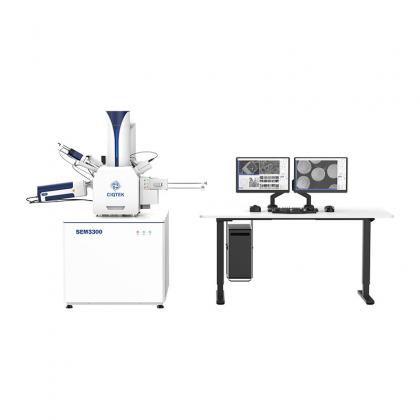
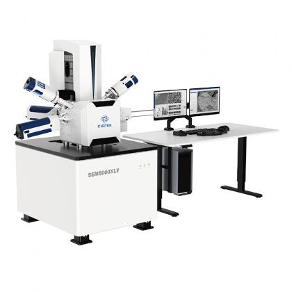
CIQTEK brings SEM and FIB together as a powerful team, providing critical support for PCB process optimization, reliability verification, and root cause determination of failures.
SEM High-Resolution Imaging: The "Microscope" for Surface Details
The SEM uses a high-resolution electron beam to capture crisp images of PCB surface morphology. It reveals solder pad plating, intermetallic compounds, micro-cracks, tin whiskers, and foreign particle contamination with exceptional clarity.
Coupled with energy-dispersive X-ray spectroscopy (EDS), the SEM also performs elemental analysis on microscopic regions. This combination lets engineers identify the chemical signature of defects, making it straightforward to spot issues like short circuits, open circuits, corrosion, and plating anomalies.
FIB Nanoscale Cutting: The "Scalpel" for Internal Structures
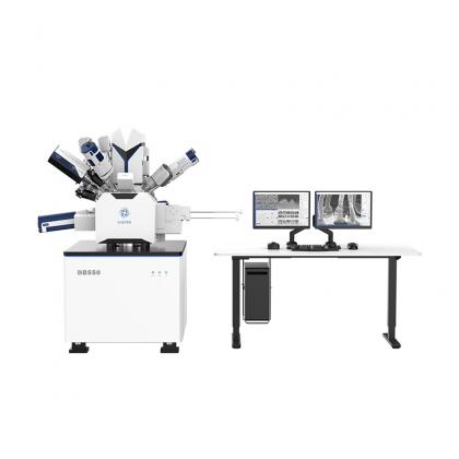
While the SEM excels at surface imaging, the FIB takes over when you need to see what is happening inside the board. Using a nanometer-precision ion beam, the FIB performs targeted cross-sectioning at the exact defect location. It prepares ultra-thin slices through multi-layer boards, blind vias, and buried vias, exposing internal structures that mechanical sectioning simply cannot reach.
Think of the FIB as a microscopic surgical tool. It removes material with nanometer accuracy, leaving a clean cross-section ready for imaging and analysis.
CIQTEK Semiconductor Showcase: See It in Action
The Beauty of the Microscopic World, Revealed in Every Detail.
Here are real examples of CIQTEK electron microscopes in PCB cross-section observation:
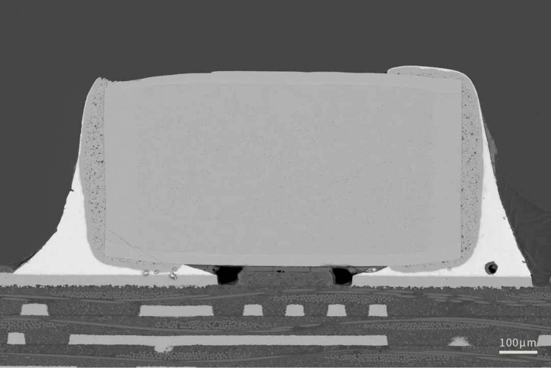
Solder Joint Interface Panorama
Low magnification observation of capacitor overall morphology, viewing the real microscopic structure of the capacitor solder joint interface from the inside
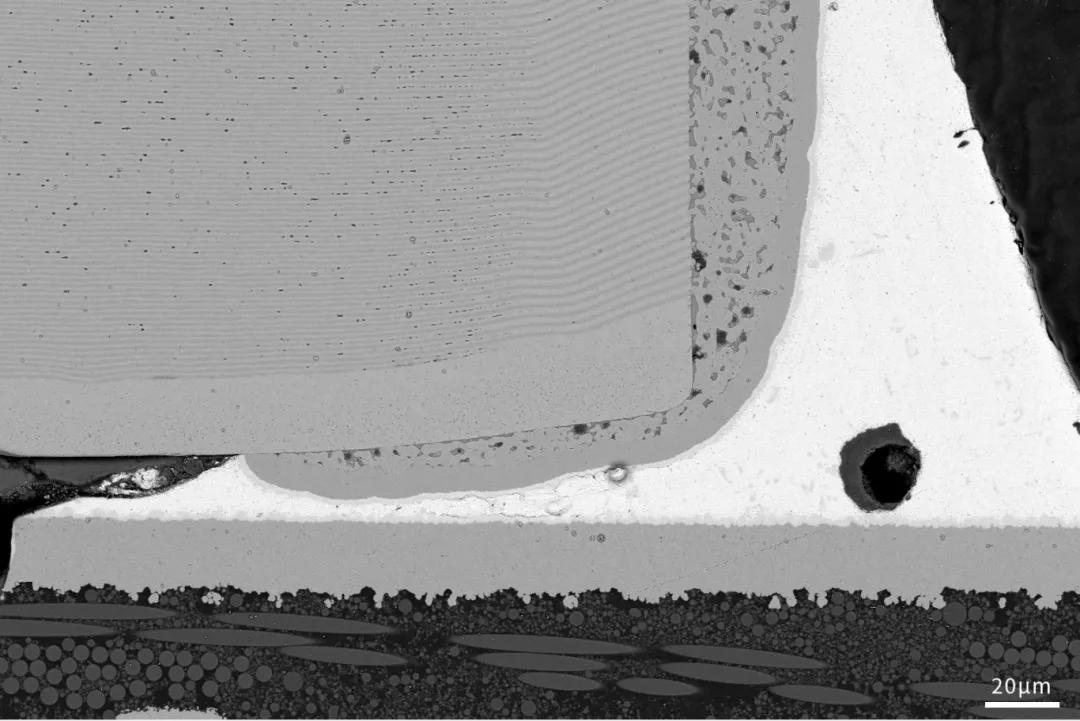
IMC Layer Evaluation
Evaluating interlayer bonding, measuring IMC thickness and uniformity, detecting voids, cracks, and interface defects
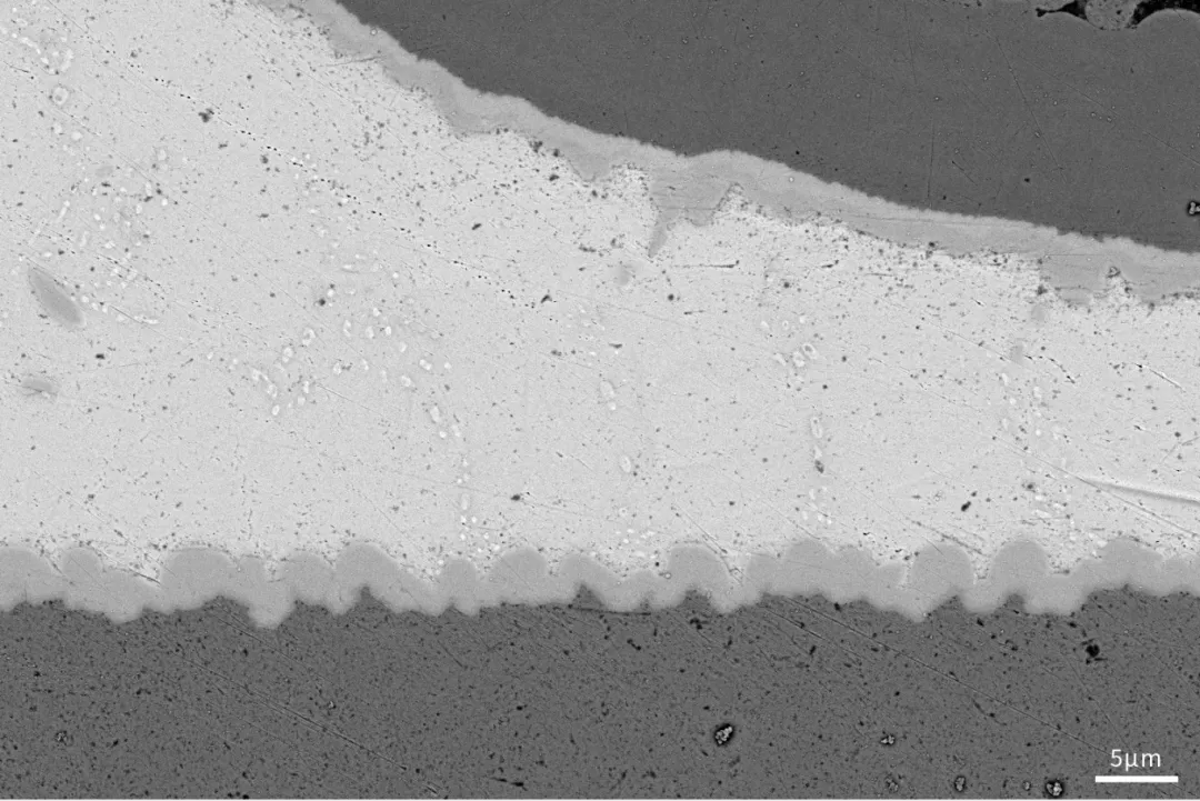
Multi-Layer Board Inner Structure
Clear observation of IMC layer morphology, thickness, continuity, and density at the solder pad and solder interface
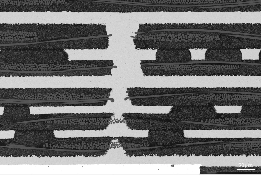
Process Reliability Evaluation
Evaluating trace pattern, thickness, etching quality and copper-to-substrate bonding, detecting line shift, etch defects, delamination, voids, and analyzing plating layer quality for PCB process control and reliability assessment
Built for Labs That Demand Reliability
CIQTEK develops its electron microscopy platforms from the ground up, covering core algorithms through hardware design. This vertical integration ensures consistent performance and long-term supply stability, which matters for labs running continuous production or multi-year research programs.
The company backs its instruments with responsive technical support and regular software updates, helping users keep their systems running efficiently over time.
Get in Touch
If you are evaluating SEM or FIB systems for your PCB inspection workflow, the CIQTEK team can help you identify the right configuration for your application.
Пожалуйста, не стесняйтесь обращаться к нам для получения более подробной информации, запроса ценового предложения или заказа онлайн-демонстрации! Мы ответим вам, как только сможем.